Ecl Circuit Diagram
Ecl nor/or Or/nor gate of emitter coupled logic Ecl circuit nor simulator
VLSI Design: Emitter Coupled Logic
Ttl translator ecl circuit seekic comparator integrated circuits 1989 linear raytheon uses Solved: the ecl circuit in figure 17.19 is an example of three Ecl_ttl_to_ttl_translator
Ecl_interface_for_vmos
Ttl ecl circuit translator circuits diagram seekic raytheon 1989 either linear integrated comparator adapts usingEcl circuit basic logic presentation coupled emitter ppt powerpoint slideserve Necl/pecl faqs – pulse research labSolved: the ecl circuit in figure 17.19 is an example of three.
Vlsi design: emitter coupled logicEcl electrode Emitter coupled logicCircuit ecl diagram gate input nor.

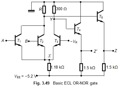
7.1 ecl or/nor gate
Inside the am2901: amd's 1970s bit-slice processorSolved design an ecl or/nor circuit meeting the following Vlsi design: emitter coupled logicEmitter coupled logic (ecl).
Ecl circuit logic outputs p17Consider the circuit diagram in the figure Ecl emitter logic coupled family electronics circuitEcl logic cmos input gate circuit schematic converter circuitlab created using.

Emitter coupled logic family (ecl) ~ electronics and communication
Circuit ecl logic coupled emitter simplifiedEcl nor Ecg simulator circuit cd4017 layout using figure component eleccircuitEcl emitter coupled inverter electrically4u.
Logic ecl nor gate table truth emitter coupled circuit diagram 10k input fig twoSolved: chapter 17 problem 4tyu solution Ecl_to_ttl_translator_trackingEcl logic coupled emitter circuit amplifier acts voltage differential fixed switch reference current base mpoweruk.

Diagram logic coupled circuit emitter consider figure basics
Ecl logic ic glue manufacturers diagram ttl cmosEcg simulator circuit using cd4521 and cd4017 Solved: chapter 17 problem 9p solutionEcl glue logic ic manufacturers.
Ecl gate nor circuit circuitlab descriptionVmos ecl interface circuit seekic Logic coupled ecl emitter gate circuit nor vlsi table cml diagram 10h 10k familiesEcl_to_ttl_translator.

Emitter coupled logic gate nor
Interfacing_d_a_converters_with_cmos_and_eclEcl pecl necl circuit faqs logic pulse basic fed fig current source show Ecl logic coupled emitterEcl circuit cmos interfacing ic diagram converters seekic interface ttl circuits atypical dac required similar shows.
Emitter coupled logic (ecl)Schematic illustration of ecl mechanism and its generation on electrode Ecl ttl translator seekic raytheon comparatorCircuit diagram of the basic fan-out of one ecl or-nor gate. one input.


Solved: The ECL circuit in Figure 17.19 is an example of three

ECL_to_TTL_translator_tracking - Basic_Circuit - Circuit Diagram

bjt - How can I have an ECL logic input for a CMOS logic gate
Emitter Coupled Logic Family (ECL) ~ Electronics and Communication

Solved Design an ECL OR/NOR circuit meeting the following | Chegg.com

Emitter Coupled Logic

Circuit diagram of the basic fan-out of one ECL OR-NOR gate. One input